Assessment Result
Your assess result is as shown. is where the patent is located.
The deeper the color of the map, the higher the potential value your patent may have.
Now you can choose to:
Assess Result of Patent 4793895

Current Patent Position
More About The Patent
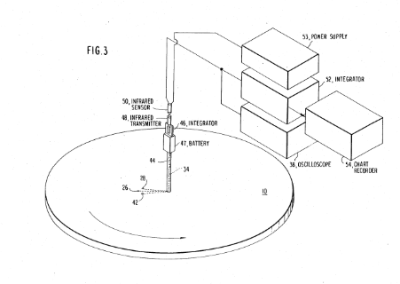
Patent ID: 4793895
Grant Date: 1988-12-27
Assignee: International Business Machines Corp
Abstract:
An apparatus and method for monitoring the conductivity of a semiconductor wafer during the course of a polishing process. A polishing pad that contacts the wafer has an active electrode and at least one passive electrode, both of which are embedded in the polishing pad. A detecting device is connected to the active and passive electrodes for monitoring the current between the electrodes as the wafer is lapped by the polishing pad. The etch endpoint of the wafer is determined as a function of the magnitude of the current flow.
Related Products:
This is one of the most valuable patents in the world. The patent royalty is more than billions of dollars per year! It became the standard for flattening in high-density semiconductor manufacturing in the 1990s.